Here students can locate TS Inter 2nd Year Physics Notes 15th Lesson Semiconductor Electronics: Material, Devices and Simple Circuits to prepare for their exam.
TS Inter 2nd Year Physics Notes 15th Lesson Semiconductor Electronics: Material, Devices and Simple Circuits
→ Classification of solids (based on resistance or conductivity)
→Metals : Solids with low resistivity (ρ) or high conductivity (σ) are called metals.
Resistivity (ρ) of metals is 10-2 – 10-8 ohm – m.
Conductivity (σ) of metals is 102 to 108 S m-1.
→ Semiconductors: For semiconductors the resistivity (ρ) and conductivity (σ) are in intermediate range.
Resistivity (ρ) is 10-5 to 106 Ω m ;
Conductivity (σ) is 105 to 10-6 S m-1.
→ Insulators : For insulators the resistivity (ρ) is very high and conductivity (σ) is very less.
Resistivity (ρ) is 1011 to 1019 Ω m ;
Conductivity (σ) is 10-11 to 10-19 Sm-1.
Note: Resistivity is not the only criteria to classify solids. Many other factors are also taken into account.
→ Semiconductors :
- In semiconductor devices the supply and flow of charge carriers are within the solid itself.
- Semiconductors are again divided into two types.
- Elemental semiconductors : Elements such as Germanium (Ge) and Silicon (Si) are called “elemental semiconductors”
- Compound semiconductors: These are again two types.
- Inorganic semiconductors such as CdS, GaAs, CdSe, InP etc.
- Organic semiconductors such as anthracene, doped pthalocyanlnes etc. and
Organic polymers such as polypyrrole, polyaniline etc.
→ Energy Bands:
- According to Bohr theory in an isolated atom the energy of any electron is decided by the orbit in which it revolves.
- When atoms come together to form a solid these energy levels will come close together or even they may overlap. As a result an electron will have different energy levels with continuous variation of energy, which leads to the concept of energy bands.
- Valence band: The energy band which incl-udes all the energy levels of valence electrons is called “valence band”.
![]()
→ Conduction band: The energy level above valence band is called “conduction band”.
If there is some gap between valence band and conduction band then electrons in valence band will be bounded and there are no free electrons in conduction band. Note : If the lowest energy level of conduction band coincides with highest energy level of valence band or if lowest energy level of conduction band is less than highest energy level of valence band then electrons can freely go to conduction band with no external energy this is the case with most of the solids.
→ Forbidden band : The energy gap between valence band and conduction band where we cannot see any electrons is called “for-bidden band”.
Note: In case of semiconductors forbidden band width is less than 3 eV. (For Germanium it is 0.7eV and for Silicon it is 1.1 eV). Because of this small gap even at room temperatures some electrons from valence band can acquire enough energy they will cross the forbidden gap and goes to conduction band due to this reason resistance of semiconductors is less.
→ Intrinsic semiconductors: Semiconductors with ultra high pure state are called “intrinsic semiconductors”.
In pure Germanium (Ge) or Silicon(Si) crystal every Germanium or Silicon atom forms four covalent bonds with neighbouring Ge/Si crystal.
At very low temperature, intrinsic semi-conductors are insulators when temperature increases electrons absorbs more thermal energy and it may become a free electron and that atom will become positive.
A free electron leaves a positive site called hole. Le., thermal energy effectively ionises a few atoms. •
In intrinsic semiconductors number of free electrons (n^ is equal to number of holes (n^) and current contribution by electrons (7J and holes (1^) is same.
∴ In an intrinsic semiconductor ne = nh = n1
Total current I = Ie + Ih
→ Extrinsic semiconductors: A suitable amount of impurity is added to intrinsic semiconductor to promote its conductivity. Such type of semiconductors are called “extrinsic semiconductors” or “impure semi-conductors”.
→ Doping: The process of deliberate addition of impurities to intrinsic semiconductor to promote conductivity is called “doping”.
→ n – type semiconductors: When pentavalent impurities such as phosphorous (P), arsenic (As), antimony (Sb) are added to intrinsic semiconductors then they are called “n-type semiconductors”.
In these semiconductors current flows through negative charges (electrons) so they are called n-type.
Note : In n-type semiconductors majority charge carriers are “electrons”, minority charge carriers are “holes”.
→ p-type semiconductors : When trivalent impurities such as Boron (B), Aluminium (Al), Galium (Ga), Indium (In) etc. are added to intrinsic semiconductor then it is called “p type semiconductor”.
In these semiconductors current flows through positive charges called holes. So they are called p-type semiconductors.
Note : In p-type semiconductors majority charge carriers are “holes” and minority charge carriers are “electrons”.
→ p-n junction : A p-n junction is formed by adding a small quantity of pentavalent impurities in a highly controlled manner to a p-type silicon/germanium wafer.
→ During the formation of p-n junction diffusion and drift of charge carriers takes place.
→ In a p-n junction concentration of holes is high at p – side and concentration of electrons is high at n-side. Due to the concentration gradient between p-type and n-type regions holes diffuse to n-region and electrons diffuse to p-region. This leads to diffusion current.
→ Due to diffusion of electron an ionised donor is developed at n-region and due to diffusion of holes to n- region an ionised acceptor will develop at p-region. These ions are immobile. So some – ve charge is developed in p-region and positive charge is developed in n-region. This space charge prevents further motion of electrons and holes near junction.
→ Depletion layer : Both the negative and positive space charge regions near junction are called “depletion region”.
→ Drift: The motion of charge carriers due to the electric field is called drift. Current flowing due to drift of charges is called “drift current*.
Note : In a p-n junction total current is the sum of diffusion current and drift current. The direction of drift current is opposite to diffusion current.
→ In a p-n junction initially diffusion current is large and drift current is small.
![]()
→ In a p-n junction under equilibrium conduction there is no net current.
→ p-n junction forward bias: When external voltage ‘V is applied to a p-n junction such thatp-region is connected to ‘+ ve’ terminal and n region is connected to ‘-ve’ terminal then it is called “forward bias”.
→ p-n junction reverse bias : When external voltage V is applied to a p-n junction such that p – region is connected to ‘- ve’ terminal and n-region is connected to ‘+ve’ terminal then it is called “reverse bias”.
→ Rectifier : The process of converting alternating current (a.c) into direct current (d.c) is called “rectification”. Instruments used for rectification is called “rectifier”.
Note : A p-n junction diode can be used as a rectifier because it allows current to flow in one direction only. i.et, in forward bias it will conduct current whereas in reverse bias it does not allow current to pass through it.
→ Zener diode : A zener diode is a highly doped p-n junction with sharp break down voltage. Generally zener is operated in reverse bias condition.
Note: In forward bias condition zener diode will also act as ordinary p-n junction.
→ Transistor : A transistor is a three layered electronic device.
These layers are called emitter, base and collector.
Transistors are two types 1) p-n-p 2) n-p-n
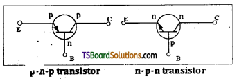
→ Emitter: Emitter region is of moderate size. It is heavily doped. It supplies large number of majority charge carriers for the current flow through transistor.
→ Base : Width of base region is very less. It is lightly doped nearly with 3 to 5% impurity concentration of emitter.
→ Collector: Size of collector region is larger than emitter. It is moderately doped (i.e., impurity concentration is less than emitter).
→ Biasing of transistor : In a transistor for transistor action to takes place
- Emitter base region must be forward biased,
- Base collector region must be reverse biased,
- Forward bias emitter base potential VEB must be Jess than reverse bias collector base potential VCB.
- If a transistor is biased as above than the transistor is said to be in active state.
→ In a transistor emitter current (IE) = Base current (IB) + Collector current (IC)
IE = IB + IC
Hence transistor is a current controlled device.
→ Input resistance (r1): It is defined as the ratio of change in emitter base voltage (ΔVBE) to change in base current (AIg) when collector-emitter voltage is constant.
Input resistance, ri = \(\left[\frac{\Delta \mathrm{V}_{\mathrm{BE}}}{\Delta \mathrm{I}_{\mathrm{B}}}\right]_{\mathrm{V}_{\mathrm{CE}}}\)
→ Output resistance (r0): It is defined as the ratio of change in collector- emitter voltage (ΔVCE) to change in collector current (Ic) when base current (IB) is constant.
Output resistance, r0 = \(\left[\frac{\Delta \mathrm{V}_{\mathrm{CE}}}{\Delta \mathrm{I}_{\mathrm{C}}}\right]_{\mathrm{I}_{\mathrm{B}}}\)
→ Current amplification factor (β): It is defined as the ratio of change in collector current (Ic) to change in base current (IB) when collector – emitter voltage (VCE) is constant.
Current amplification, β = \(\left[\frac{\Delta \mathrm{I}_{\mathrm{C}}}{\Delta \mathrm{I}_{\mathrm{B}}}\right]_{\mathrm{V}_{\mathrm{CE}}}=\frac{\mathrm{I}_{\mathrm{C}}}{\mathrm{I}_{\mathrm{B}}}\)
→ Transistor as a switch : By changing the emitter base potential a transistor can be operated as a switch. For a transistor when input emitter-base potential is less than 0.6 V it is in cut off mode i.e., output current is zero. If input Vi is more than 0.6V transistor is in active state and we will get output current.
This property of output voltage V0 is high or low is used in switches.
→ Transistor as an amplifier: A transistor can be used as an amplifier in its active region. In this region output voltage v0 increases drastically even for a small change in input voltage Vi.
In transistor amplifier the mid point of active region is taken as operating point (also called.lnput potential) on which varying signal voltage is superposed. This vanat ion is magnified at output side by a factor equak to amplification factor β.
→ Voltage amplification factor Av: ¡fis defined as the ratio of output signal voltage (V0) to in put signal voltage (Vi).
Voltage amplification, Av = \(\left[\frac{v_0}{v_i}\right]_{v_{B B}}=\beta \frac{R_C}{R_B}\)
Note : Generally voltage amplification is given at common emitter configuration VBB is emitter – base voltage in common emitter configuration.
→ Feedback amplifier : When a part of the output of an amplifier is fed as input in emitter base circuit then it is called “feed back amplifier”.
Note : Generally feedback is achieved by inductive coupling or LC or RC networks.
→ Transistor oscillator: A transistor oscillator is also a feedback amplifier with a suitable value of inductance (L) and capacitor (C) at output side. A part of output of L.C circuit is given as feedback to emitter base circuit.
Frequency of oscillation, υ = \(\frac{1}{2 \pi \sqrt{\mathrm{LC}}}\)
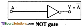
→ NOT gate : It has one input terminal and one output terminal. The output of NOT gate is the opposite of input i.e., if input is ‘O’ then output is T. If input is T then output is ‘0’.
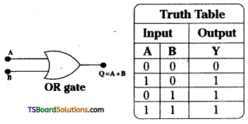
→ OR gate: It consists of two input terminals and one output terminal. In this gate if any one input terminal is high then the output is also high as shown in truth table.
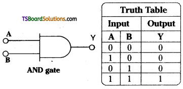
→ AND gate : It consists of two input terminals and one output terminal. In AND gate if both input signals are high (say A and B) then only output is high truth table is as shown.
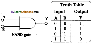
→ NAND gate: It consists of two input terminals and one output terminal. NAND gate is a combination of AND gate and NOT gate. If any one of input signal (A or B) is ‘O’ we will get T as output.
![]()
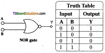
→ NOR gate : It consists of two input terminals and one output terminal. NOR gate is a combination of OR gate and NOT gate. The output is the negative of OR gate as shown in truth table.